92
9151AINDCO07/09
ATA8742
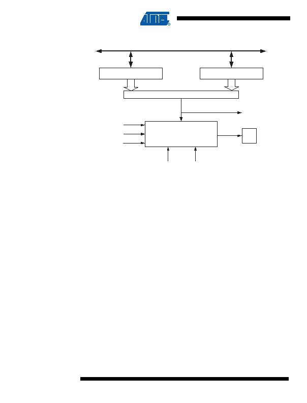
Figure 20-3. Output Compare Unit, Block Diagram
The OCR0x Registers are double buffered when using any of the Pulse Width Modulation
(PWM) modes. For the normal and Clear Timer on Compare (CTC) modes of operation, the dou-
ble buffering is disabled. The double buffering synchronizes the update of the OCR0x Compare
Registers to either top or bottom of the counting sequence. The synchronization prevents the
occurrence of odd-length, non-symmetrical PWM pulses, thereby making the output glitch-free.
The OCR0x Register access may seem complex, but this is not case. When the double buffering
is enabled, the CPU has access to the OCR0x Buffer Register, and if double buffering is dis-
abled the CPU will access the OCR0x directly.
20.5.1
Force Output Compare
In non-PWM waveform generation modes, the match output of the comparator can be forced by
writing a one to the Force Output Compare (0x) bit. Forcing Compare Match will not set the
OCF0x Flag or reload/clear the timer, but the OC0x pin will be updated as if a real Compare
Match had occurred (the COM0x1:0 bits settings define whether the OC0x pin is set, cleared or
toggled).
20.5.2
Compare Match Blocking by TCNT0 Write
All CPU write operations to the TCNT0 Register will block any Compare Match that occur in the
next timer clock cycle, even when the timer is stopped. This feature allows OCR0x to be initial-
ized to the same value as TCNT0 without triggering an interrupt when the Timer/Counter clock is
enabled.
20.5.3
Using the Output Compare Unit
Since writing TCNT0 in any mode of operation will block all Compare Matches for one timer
clock cycle, there are risks involved when changing TCNT0 when using the Output Compare
Unit, independently of whether the Timer/Counter is running or not. If the value written to TCNT0
equals the OCR0x value, the Compare Match will be missed, resulting in incorrect waveform
OCFnx (Int.Req.)
= (8-bit Comparator )
OCRnx
OCnx
DATA BUS
TCNTn
W Mn1:
Waveform Generator
top
FOCn
MnX1:
bottom
发布紧急采购,3分钟左右您将得到回复。
相关PDF资料
ATA8743-PXQW
MCU W/TRANSMITTER ASK/FSK 24QFN
ATAVRRZ200
KIT DEMO AT86RF230
AV101-12LF
ATTENUATOR HIP3 0.70-1GHZ 8-SOIC
AV102-12LF
ATTENUATOR HIP3 1.7-2GHZ 8SOIC
AV113-12LF
ATTENUATOR HIP3 2.1-2.3GHZ 8SOIC
AXUV100G
SENSOR ELECTRON DETECTION
B0205F50200AHF
XFRMR BALUN RF 200-500MHZ 1608
B0310J50100AHF
XFRMR BALUN RF 300-1000MHZ 0805
相关代理商/技术参数
ATA8743
制造商:ATMEL 制造商全称:ATMEL Corporation 功能描述:Microcontroller with UHF ASK/FSK Transmitter
ATA8743C- PXQW
功能描述:8位微控制器 -MCU Embedded uC incl RF Tx for 315 MHz
RoHS:否 制造商:Silicon Labs 核心:8051 处理器系列:C8051F39x 数据总线宽度:8 bit 最大时钟频率:50 MHz 程序存储器大小:16 KB 数据 RAM 大小:1 KB 片上 ADC:Yes 工作电源电压:1.8 V to 3.6 V 工作温度范围:- 40 C to + 105 C 封装 / 箱体:QFN-20 安装风格:SMD/SMT
ATA8743C-PXQW
制造商:Atmel Corporation 功能描述:EMBEDDED ?C INCL RF TX FOR 868 MHZ - Trays 制造商:Atmel Corporation 功能描述:EMBEDDED C INCL 868MHZ TX
ATA8743C-PXQW-1
功能描述:EMBEDDED INCL RF TX FOR 868 MHZ 制造商:microchip technology 系列:- 包装:剪切带(CT) 零件状态:在售 频率:868MHz ~ 928MHz 应用:通用 调制或协议:UHF 数据速率(最大值):32kbps 功率 - 输出:5.5dBm 电流 - 传输:9.8mA 数据接口:SPI 天线连接器:PCB,表面贴装 存储容量:4kB 闪存,256B EEPROM,256B SRAM 特性:- 电压 - 电源:2 V ~ 4 V 工作温度:-40°C ~ 85°C 封装/外壳:24-VQFN 裸露焊盘 标准包装:1
ATA8743-PXQW
功能描述:8位微控制器 -MCU Embedded uC incl RF Tx for 315 MHz
RoHS:否 制造商:Silicon Labs 核心:8051 处理器系列:C8051F39x 数据总线宽度:8 bit 最大时钟频率:50 MHz 程序存储器大小:16 KB 数据 RAM 大小:1 KB 片上 ADC:Yes 工作电源电压:1.8 V to 3.6 V 工作温度范围:- 40 C to + 105 C 封装 / 箱体:QFN-20 安装风格:SMD/SMT
ATAB5275
功能描述:射频开发工具 LF Tx Antenna driver board (TPMS) RoHS:否 制造商:Taiyo Yuden 产品:Wireless Modules 类型:Wireless Audio 工具用于评估:WYSAAVDX7 频率: 工作电源电压:3.4 V to 5.5 V
ATAB5276
功能描述:射频开发工具 1A Antenna Driver Demoboard RoHS:否 制造商:Taiyo Yuden 产品:Wireless Modules 类型:Wireless Audio 工具用于评估:WYSAAVDX7 频率: 工作电源电压:3.4 V to 5.5 V
ATAB5278
功能描述:射频开发工具 LF Tx Antenna driver board (PEG) RoHS:否 制造商:Taiyo Yuden 产品:Wireless Modules 类型:Wireless Audio 工具用于评估:WYSAAVDX7 频率: 工作电源电压:3.4 V to 5.5 V